Multi function Transverter interface board
Winner of the Scottish Microwave Round Table (GMRT) construction contest 2024.
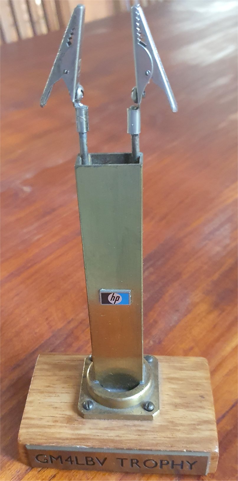
The infamous 'Wave-guide to crocodile clip adaptor'
Page under construction!!
I have a number of SHF transverter projects waiting to be finished and they all lack one thing... an interface to the driving IF transceiver
In the past I have built bespoke interfaces and no 2 are the same. There are some core functions and then some equipment specific requirements
I have now designed a 'universal' transverter interface (others have done similar in the past but I haven't seen any available that meet my requirements)
Having the PCBs made (and partially populated with the small SMD components) is quite cost effective.
The design (Still a work in progress) has evolved to include quite a few features and is not quite as simple as I originally envisaged
This has resulted in a moderately high component count. My PCB house of choice, JLCPCB, has a good stock of components and can populate one side of a board in the factory
Some of the components have a moderate price tag (eg the ERA-3+ MMIC, the power SMD resistors and the hexfet switching devices
The resultant cost is still reasonable when spread over multiple boards
Because of the board size contstraints (for a couple of my projects), the component densityis high so a number of SMD components are needed on the rear of the PCB. These will have to be fitted by hand
initial estimate of a per board cost based on a production run of 10 is about £20 each, additional components will add a few pounds, I can purchase from Mouser etc to complete the kits
Of course not all components will be needed for some configurations
Components on the front of the board are typically 0603 size, those on the rear that have to be hand soldered are mostly 0805 or SOT23
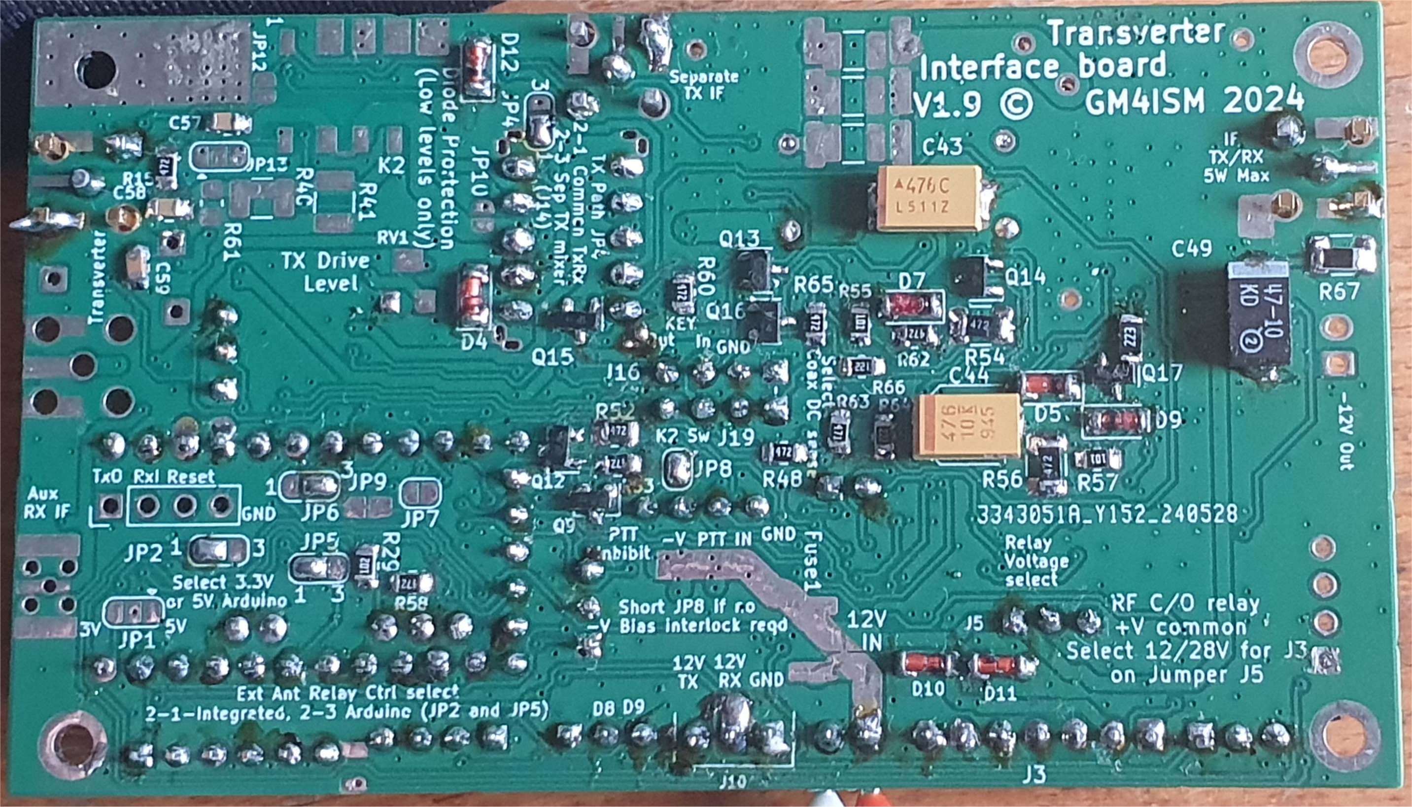
Update -- Further features added 2nd April!. Design is now at V1.9
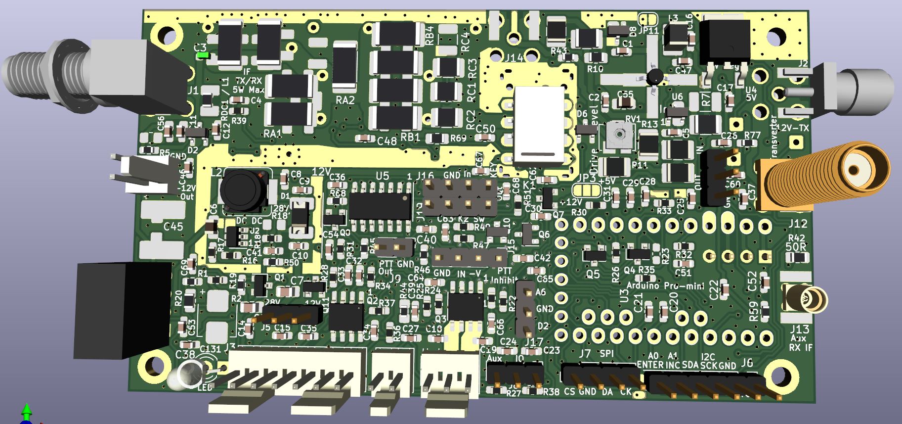
![]()
Features so far include
12-14V DC in
IF rig RF interface with built in power attenuator (max about 5W)
Designed for IF of 28MHz to 432 MHz .. See prototype notes
Attenuators can be configured for different TX powers and Transverter input requirements
The main input attenuator will be 10dB but by changing resistors, it can easily be set to 6dB
The secondary TX only attenuator is adjustable / can be configured with the idea that with 5W in you can present the mixer with less than 1mW if needed or up to 500mW
The nominal minimum attenuation of this section will probably be set to 10dB as supplied, giving 50mW or less to the TX mixer. For referemnce the G4DGU transverter wants +10dBm, a level 7 mixer would want about 0dBm
PTT processing using :-
RF detection
DC on the coax of IF rig (on TX or RX)
external PTT In
PTT is fed back out by hardware or arduino sequencer (open collector)
Another separate Sequencer output is available
On-board RF changeover relay Tx to Rx with IF amp available for RX path (as a fixed power attenuator is before on board TxRx switching)
Can be configured for separate Tx and Rx mixers, or common mode.
A MMIC based receive IF amplifier. There is a moderate amount of fixed attenuation inherent in the design and it also allows
a separate buffered receive only IF output. This is terminated in an accessible 47 Ohm 0805 resistor as supplied
Several different MMIC footprints are combined and provision is made on the PCB for a small fixed 5V regulator for the types that need this.
A basic sequencer is integrated to provides a delayed +12V TX supply after Antenna Relay is moved and remove this 12V before the relay is de-energised
Sequencer timings are hard wired but larger SMD components used here make these user 'adjustable'
-Ve supply detection to inhibit TX12V and PTT (can be disabled with a link)
external interlock PTT inhibit
A +12V supply on RX only
External antenna relay switching for either fail-safe or latching relays with a +28V DC-DC converter built in for 28V relays. The voltage can be lowered by adding an extra 0805 resistor to a position provided
PTT and therefore +12V TX can be inhibited on loss of external -V supply, or with a closed contact to allow for fil delays over temperature trips, external changeover back contacts etc
Morse Key input can trigger the PTT (with pre-set hang time) but wont pass the keying back out (to the transceiver) until 12V TX power for the transverter is applied by sequencer.
Optional on-board arduino pro-mini that can be used for more sophisticated sequencing & control, its primary purpose for me is a PLL code loader for the LO.
It could also load a different freq between Tx and Rx. All spare IO is presented
Board also supports an integrated 1W DC-DC converter to output -12V at 80mA for bias of PAs etc
PCB is configured for both vertical and side mounted SMA RF connectors (except for the Aux IF out, which due to space constraints is edge mount SMA or MMCX)
PCB supports several relay types, including a thru hole version for the main relay (tiny holes need to be enlarged). Jumpers allow the selection of 5V or 12V for the relay coil voltage
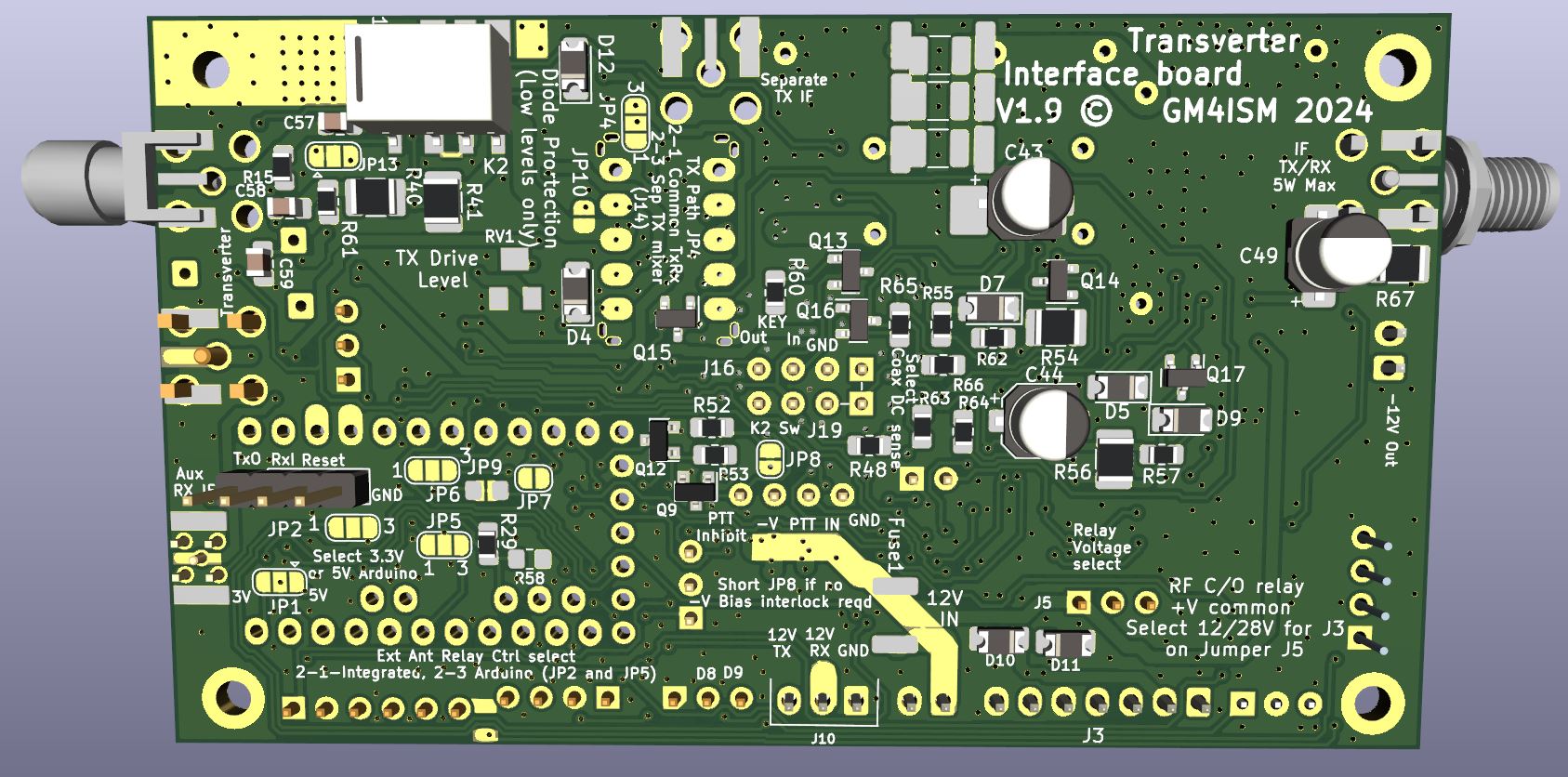
***** EXTRA FEATURE *****
At the request of 2 possible users I have added an extra feature. The board will have another RF output port for a second transverter.
An additional relay can be manually fitted and band switching input has been implemented. There are connections for a switched 12V supply on the board (no header as there is no room).
PTT, power and relay switching etc lines to the separate transverters will have to be done externally. The secondary port has provision for an extra attenuator
so that if the 2 transverters require slightly different RF levels, this can be accommodated
DC on coax PTT switching provisioned for the transverters
Layout slightly revised so that the PCB can be mounted upside down, allowing easier access to most of the jumpers, drive pot and Adjust On Test components (eg sequencer timings)
***** Initial testing *****
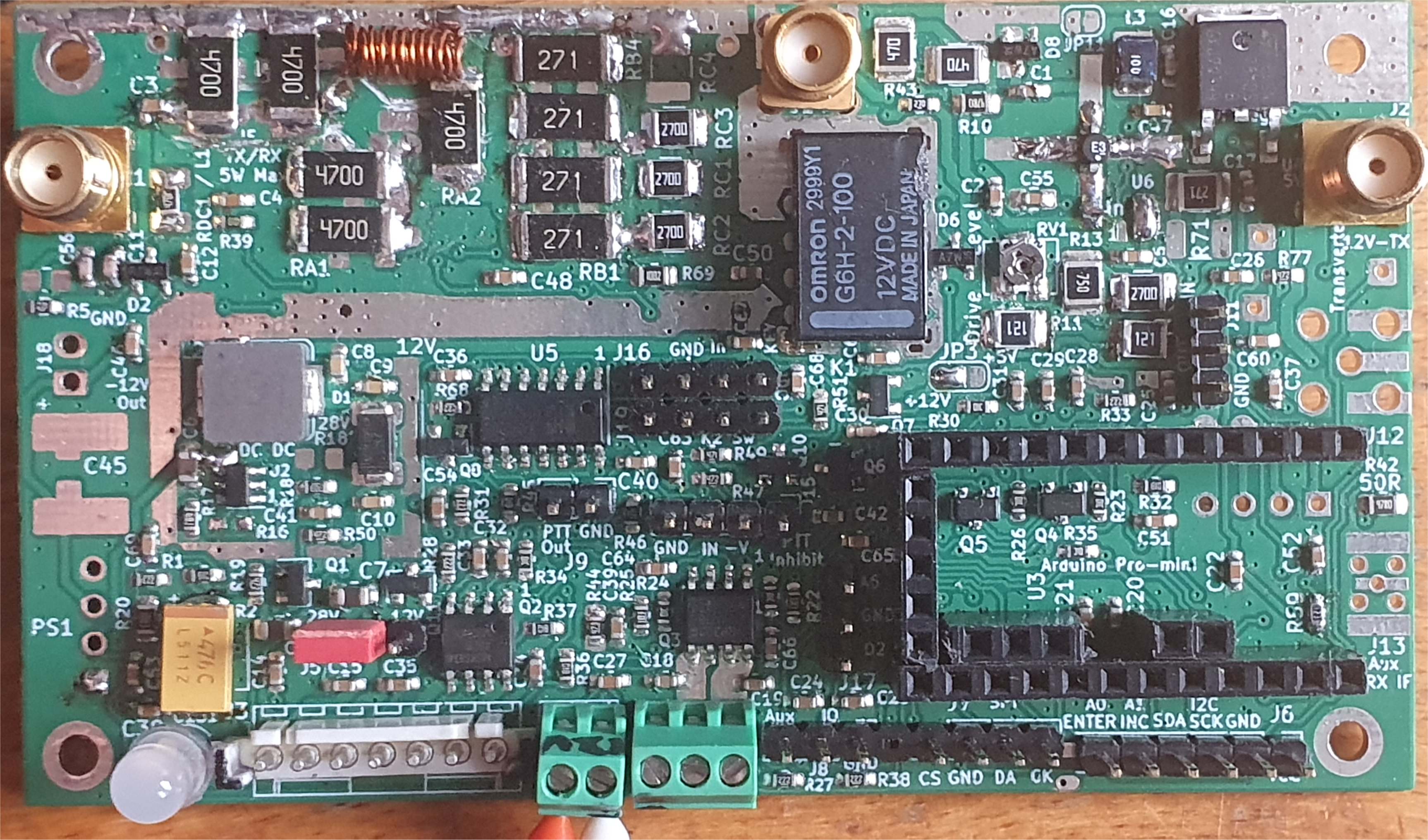
10 prototype boards, partially populated have now been received and are being evaluated.
The first board has been pretty much fully populated. All PTT functions and hardware sequencer tested and working as expected .
The attenuator input match is OK at 28MHz but degrades at higher frequency more rapidly than I had hoped. To get a good match above 70MHz, the extra stray capacitance associated with a multiple SMD resistor attenuator have to be tuned out.
A small inductor in parallel with the input resistors does this nicely but makes the input match a little more narrowband.
A different value is needed to tune for a 70cm IF. So far, performance with only a 2m IF has been evaluated
RF Detection PTT sensitivity measured at +14dBm on 145MHz. Input return loss >20dB over 140-150MHz
Main antenna relay switching tested with a 28V Spinner latching coaxial relay. This requires a brief pulse at about 600mA (it self disconnects) Reliable operation achieved from the inbuilt 28V DC-DC converter
Sequencer timings have not been measured accurately but nominal delays are seen and heard. Default delays are quite long, it is easy to change component values if you desire shorter (or longer) delays
External PTT inputs, inhibit, and -ve supply detection all worked out of the box
CW keying didn't! on close examination it seems I missed out 1 resistor in the schematic. 1 track needed to be cut and a 22K resistor (designated R3) placed. Not hard to do and all boards will be modified.
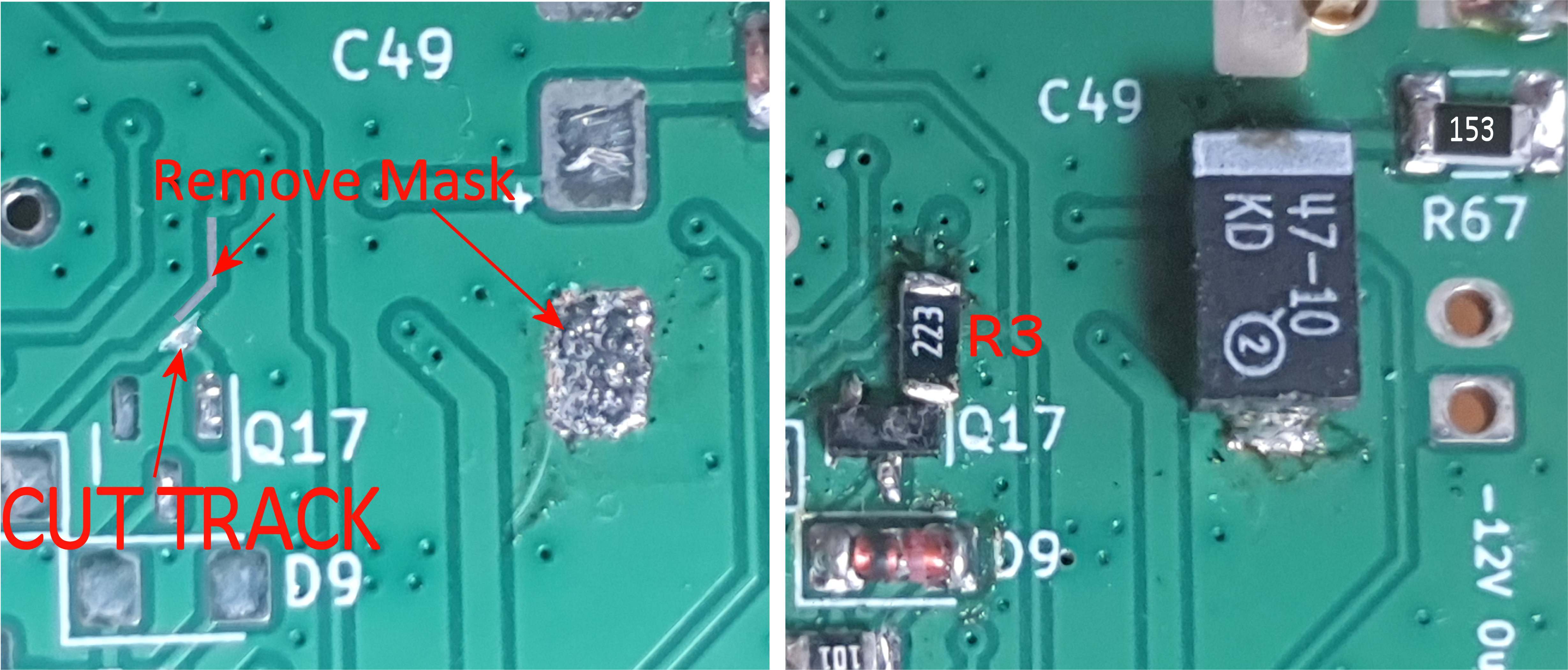
The schematic above has been upodated to show the changes.
I also had to rotate a capacitor (CW Hang Timing) as it fouls one of the SMA sockets if a through hole version is used. Again an easy modification, all V1.9 PCBs will be modified.
These changes have been incorporated into V2.0 if demand is sufficient to have another batch produced. Any V1.9 boards that I sell will be supplied modified.
With 2W input the attenuator does not get noticeably warm
The level out to the mixer is adjustable from about 0dBm down to less than -40dBm. a little more may be required by many transverters so I plan to modify the second (variable) attenuator and it will be supplied with a lower intrinsic attenuation
Pictures below from KiCad showing the simulated board with components. Please note the board is not gold plated :).
NOTE This is a work in progress. Component values etc. may change after evaluation of performance!.
![]()
Page under construction
Back to the Amateur Radio page
